


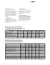
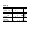


19
expressed as a percentage. With the
transmitter driven by a 25 MBd
(12.5 MHz square-wave) input
signal, the average optical power is
measured. The data “1” peak power
is then calculated by adding 3dB to
the measured average optical power.
The data “0” output optical power is
found by measuring the optical
power when the transmitter is
driven by a logic “0” input. The
extinction ratio is the ratio of the
optical power at the “0” level
compared to the optical power at the
“1” level expressed as a percentage
or in decibels.
11. The transmitter will provide this low
level of Output Optical Power when
driven by a logic “0” input. This can
be useful in link troubleshooting.
12. The relationship between Full Width
Half Maximum and RMS values for
Spectral Width is derived from the
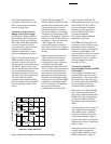
assumption of a Gaussian shaped
spectrum which results in a 2.35 X
RMS = FWHM relationship.
13. The optical rise and fall times are
measured from 10% to 90% when
the transmitter is driven by a 25
MBd (12.5 MHz square-wave) input
signal. The ANSI T1E1.2 committee
has designated the possibility of
defining an eye pattern mask for the
transmitter optical output as an
item for further study. Agilent will
incorporate this requirement into
the specifications for these products
if it is defined. The HFBR-5204 and
HFBR-5205 products typically
comply with the template require-
ments of CCITT (now ITU-T) G.957
Section 3.2.5, Figure 2 for the STM-
1 rate, excluding the optical receiver
filter normally associated with
single mode fiber measurements
which is the likely source for the
ANSI T1E1.2 committee to follow in
this matter.
14. Systematic Jitter contributed by the
transmitter is defined as the com-
bination of Duty Cycle Distortion
and Data Dependent Jitter.
Systematic Jitter is measured at
50% threshold using a 155.52 MBd
(77.5 MHz square-wave), 2
7
- 1
psuedorandom data pattern input
signal.
15. Random Jitter contributed by the
transmitter is specified with a
155.52 MBd (77.5 MHz square-
wave) input signal.
16. This specification is intended to
indicate the performance of the
receiver section of the transceiver
when Input Optical Power signal
characteristics are present per the
following definitions. The Input
Optical Power dynamic range from
the minimum level (with a window
time-width) to the maximum level is
the range over which the receiver is
guaranteed to provide output data
with a Bit Error Ratio (BER) better
than or equal to 1 x 10
-10
.
• At the Beginning of Life (BOL)
• Over the specified operating
temperature and voltage ranges
• Input is a 155.52 MBd, 2
23
- 1
PRBS data pattern with 72 “1”s
and 72 “0”s inserted per the
CCITT (now ITU-T) recommenda-
tion G.958 Appendix I.
• Receiver data window time-width
is 1.23 ns or greater for the clock
recovery circuit to operate in. The
actual test data window time-
width is set to simulate the effect
of worst case optical input jitter
based on the transmitter jitter
values from the specification
tables. The test window time-
widths are as follows: HFBR-5203
is 4.4ns, HFBR-5205 and HFBR-
5204 are 3.32 ns.
• Transmitter operating with a
155.52 MBd, 77.5 MHz square-
wave, input signal to simulate
any cross-talk present between
the transmitter and receiver
sections of the transceiver.
17. All conditions of Note 16 apply except
that the measurement is made at
the center of the symbol with no
window time-width.
18. Systematic Jitter contributed by the
receiver is defined as the combina-
tion of Duty Cycle Distortion and
Data Dependent Jitter. Systematic
Jitter is measured at 50% threshold
using a 155.52 MBd (77.5 MHz
square-wave), 2
7
- 1 psuedorandom
data pattern input signal.
19. Random Jitter contributed by the
receiver is specified with a 155.52
MBd (77.5 MHz square-wave) input
signal.
20. This value is measured during the
transition from low to high levels of
input optical power.
21. This value is measured during the
transition from high to low levels of
input optical power.
22. The Signal Detect output shall be
asserted within 100 µs after a step
increase of the Input Optical Power.
23. Signal detect output shall be de-
asserted within 350 µs after a step
decrease in the Input Optical Power.
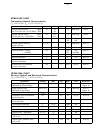
24. The HFBR-5205 transceiver
complies with the requirements for
the tradeoffs between center wave-
length, spectral width, and rise/fall
times shown in Figure 9. This figure
is derived from the FDDI PMD
standard (ISO/IEC 9314-3 : 1990
and ANSI X3.166 - 1990) per the
description in ANSI T1E1.2 Revision
3. The interpretation of this figure is
that values of Center Wavelength
and Spectral Width must lie along
the appropriate Optical Rise/Fall
Time curve.